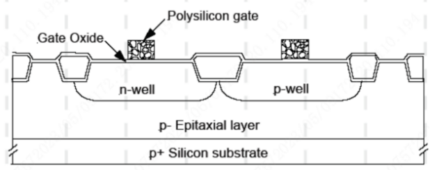
Oxidation reaction is one of the fundamental processes in semiconductor chip fabrication. It is an additive process that involves introducing oxygen into silicon wafers to form a thin layer of silicon dioxide on the wafer surface. This thin film is formed at high temperatures and is therefore also known as "thermal oxidation."
Silicon readily reacts with oxygen, which is why silicon is mostly found in the form of silicon dioxide in nature, such as quartz sand. Silicon quickly reacts with oxygen (water vapor) to form silicon dioxide on the silicon surface, which can be represented by the following reactions:
Si + O2 -> SiO2
Si + H2O -> SiO2 + H2
Silicon dioxide is a dense material that can cover the entire silicon surface. In order to continue the oxidation process, oxygen molecules must diffuse through the oxide layer to react with the silicon atoms underneath. Growing a thick silicon dioxide layer hinders the diffusion of oxygen, slowing down the oxidation process. When a bare silicon wafer comes into contact with the atmosphere, it immediately reacts with oxygen or moisture in the air to form a thin layer of silicon dioxide, approximately 10-20 angstroms thick. This is known as the native oxide layer, and at room temperature, this thin silicon dioxide layer can prevent further oxidation of silicon. The illustration below shows the oxidation process.
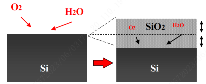
In the oxidation process, oxygen is a gas, while silicon comes from the solid substrate. Therefore, when growing silicon dioxide, silicon from the substrate is consumed, and the thin film grows inward towards the silicon substrate. The high temperature in the process enhances the movement of oxygen molecules and facilitates their diffusion through the already-formed oxide layer to react with silicon, leading to the growth of thicker silicon dioxide. The higher the temperature, the faster the movement of oxygen molecules and the faster the growth rate of the oxide film. High-temperature growth of oxide films results in higher quality compared to low-temperature growth. Therefore, in order to obtain high-quality oxide films and faster growth rates, the oxidation process must be carried out in high-temperature environments, typically within quartz (or silicon carbide) furnaces. Oxidation is a slow process and can take several hours to grow an oxide layer with a thickness of approximately 5000 angstroms, even in high-temperature furnaces exceeding 1000℃. Therefore, the oxidation process is usually conducted in batches, simultaneously processing 50-200 wafers to achieve reasonable yield.
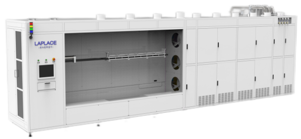
The oxidation process of silicon is one of the fundamental processes in the entire IC (integrated circuit) fabrication. Silicon dioxide has numerous applications:
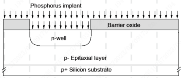
It is used as a protective oxide layer to prevent silicon contamination during the application of photoresist. It can also be used to scatter ions before they enter the single-crystal silicon, reducing channeling effects.
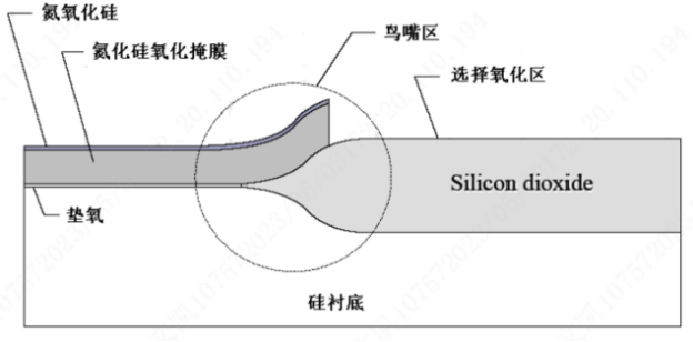
It serves as a buffer oxide layer to reduce the stress between silicon and LPCVD silicon nitride. Without a silicon dioxide buffer layer to alleviate the stress, the tensile stress of LPCVD silicon nitride layer, reaching up to 1010 dyn/cm2, could cause cracks or even fracture in the silicon wafer.
It is used as a gate oxide layer, which acts as a dielectric layer in MOSFET to facilitate current flow and provide a dielectric for field control.

Back
Silicon readily reacts with oxygen, which is why silicon is mostly found in the form of silicon dioxide in nature, such as quartz sand. Silicon quickly reacts with oxygen (water vapor) to form silicon dioxide on the silicon surface, which can be represented by the following reactions:
Si + O2 -> SiO2
Si + H2O -> SiO2 + H2
Silicon dioxide is a dense material that can cover the entire silicon surface. In order to continue the oxidation process, oxygen molecules must diffuse through the oxide layer to react with the silicon atoms underneath. Growing a thick silicon dioxide layer hinders the diffusion of oxygen, slowing down the oxidation process. When a bare silicon wafer comes into contact with the atmosphere, it immediately reacts with oxygen or moisture in the air to form a thin layer of silicon dioxide, approximately 10-20 angstroms thick. This is known as the native oxide layer, and at room temperature, this thin silicon dioxide layer can prevent further oxidation of silicon. The illustration below shows the oxidation process.

In the oxidation process, oxygen is a gas, while silicon comes from the solid substrate. Therefore, when growing silicon dioxide, silicon from the substrate is consumed, and the thin film grows inward towards the silicon substrate. The high temperature in the process enhances the movement of oxygen molecules and facilitates their diffusion through the already-formed oxide layer to react with silicon, leading to the growth of thicker silicon dioxide. The higher the temperature, the faster the movement of oxygen molecules and the faster the growth rate of the oxide film. High-temperature growth of oxide films results in higher quality compared to low-temperature growth. Therefore, in order to obtain high-quality oxide films and faster growth rates, the oxidation process must be carried out in high-temperature environments, typically within quartz (or silicon carbide) furnaces. Oxidation is a slow process and can take several hours to grow an oxide layer with a thickness of approximately 5000 angstroms, even in high-temperature furnaces exceeding 1000℃. Therefore, the oxidation process is usually conducted in batches, simultaneously processing 50-200 wafers to achieve reasonable yield.

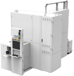
Wafer Size: 4, 6 inches
Process Types: Dry oxidation, wet oxidation (optional)
Applicable Materials: Silicon Carbide
Application Areas: Power semiconductors, research

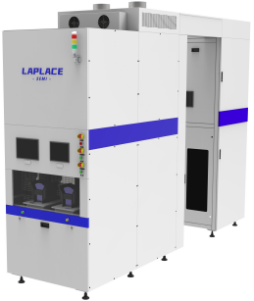
Wafer Size: 8 inches
Process Types: Dry oxidation, wet oxidation,radical oxidation, high-temperature anneal
Applicable Materials: Silicon
Application Areas: Power semiconductors, Integrated Circuits, substrate materials, research

Wafer Size: 8 inches and below
Process Types: Oxidation,anneal, alloy, LPCVD (Low-Pressure Chemical Vapor Deposition)
Applicable Materials: Silicon, Silicon Carbide
Application Areas: Power semiconductors, optoelectronic devices, research
The oxidation process of silicon is one of the fundamental processes in the entire IC (integrated circuit) fabrication. Silicon dioxide has numerous applications:
It is used as a protective oxide layer to prevent silicon contamination during the application of photoresist. It can also be used to scatter ions before they enter the single-crystal silicon, reducing channeling effects.

It serves as a buffer oxide layer to reduce the stress between silicon and LPCVD silicon nitride. Without a silicon dioxide buffer layer to alleviate the stress, the tensile stress of LPCVD silicon nitride layer, reaching up to 1010 dyn/cm2, could cause cracks or even fracture in the silicon wafer.

It is used as a gate oxide layer, which acts as a dielectric layer in MOSFET to facilitate current flow and provide a dielectric for field control.
